Professional Equipment Manufacturer


 Esperanto
 Shqiptare
 Euskara
 Zulu
Zulu
 Latinus
 Cymraeg
 தமிழ்
தமிழ்
 Slovak
 Slovak
 Afrikaans


BGA Failure Analysis
2024-01-11
Due to a significant proportion of BGA IC damage in the production process of LCD products in the early stage, and the limited analytical ability of BGA packaged ICs in our company, we contacted the Analysis Center of the Fifth Research Institute of the Ministry of Electronic Information Industry of China in late February 2005, entrusting them to analyze the soldering and failure analysis of BGA for our company. This commissioned work was completed in mid May, and we were provided with soldering and internal failure analysis of BGA chips. We organized this summary and learning meeting on the analysis report, analysis methods, and analysis situation presented. The discussion content during the meeting is recorded as follows:
1. In the welding analysis section, five analysis centers conducted a series of analyses on BGA welding:
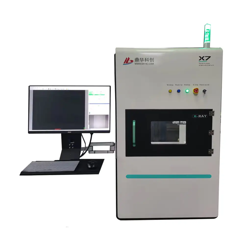
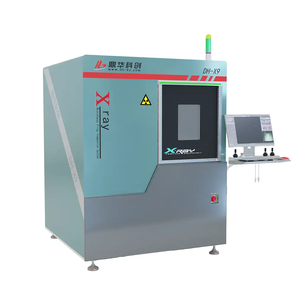
a、Firstly, they used X-ray analysis to confirm whether there were bridge connections, solder leaks, and obvious virtual soldering in the soldering of BGA chips. The results showed that there were only many voids in the solder joints, and no obvious welding defects such as bridge connections, solder leaks, or virtual soldering were observed;
b、 Then, five destructive dye penetration tests were conducted for analysis. Dye materials were injected into the chip and motherboard, and the chip and motherboard were separated. The solder joints were observed and analyzed using a stereo microscope, and it was found that both samples had less than 50% dye penetration, but it did not affect the connection performance of the solder joints;
c、 Finally, two samples were selected for metallographic section analysis (using the same destructive analysis method). The chip and motherboard were encapsulated with epoxy resin and polished with sandpaper. After cleaning, they were observed and analyzed using a metallographic microscope. It was found that there were a few solder joints with varying sizes of voids, but no obvious cracking was observed, which had no effect on the connection performance of the solder joints.
In summary, there are no significant issues with BGA soldering and it does not affect the performance of BGA usage.
2. After completing the soldering analysis of BGA in the internal analysis section of the chip, the five analysis centers conducted an internal analysis of BGA:
a、 External visual inspection was conducted on the 5 defective BGA ICs we provided, and pictures were taken without any abnormalities found;
b、 Conduct port characteristic testing, select 3 defective ICs and compare them with the good quality ICs we provide to test the port volt ampere characteristics of BGA, and no abnormalities were found;
c、 Using an acoustic scanning microscope to compare and observe defective and good products, no abnormalities were found;
d、 Afterwards, chemical opening and internal inspection were carried out, and it was observed that there were many interlayer local breakdowns between the multi-layer metalized wiring inside the BGA chip. The main cause was the breakdown between the power and ground lines and other signal lines below, resulting in constant high or low signal line levels, leading to the failure of the BGA chip.
The results of the internal analysis of the chip indicate that the failure of BGA is due to the phenomenon of interlayer local breakdown inside the chip, and the inference of the cause of this interlayer local breakdown phenomenon is related to the density of interlayer dielectric defects and high voltage pulses, indicating that the fundamental reason for BGA failure may be the quality problems of BGA components, or the damage of BGA caused by high voltage pulses (such as electrostatic discharge during production).
In terms of electrostatic protection, the factory has organized an improvement team since the end of 2004 to conduct electrostatic protection inspections and improvement work on the production process of LCD product ICs. The following figure shows the failure rate of BGA in the past 9 months:
From the graph, it can be seen that the BGA failure rate has shown an overall downward trend during the improvement of electrostatic protection work, especially after the LCD factory relocated to the new factory in May. This downward trend is more pronounced because a large amount of resources have been invested in electrostatic protection in the new factory, resulting in effective results (in the new factory, anti-static floors are used in the workshop, and all operators wear anti-static clothing, hats, shoes, wristbands, gloves, and other anti-static equipment for production operations). The improvement of electrostatic protection has achieved phased results and must be continuously improved to prevent damage and destruction of components caused by static electricity.
During this learning conference, the technical backbone of the LCD factory and engineers from the production technology department gathered to discuss and learn the analysis methods of BGA. They observed and studied the analysis reports and component debris left by the five institutes, gained a certain understanding of the analysis methods and steps of such highly integrated ICs, and once again clarified the importance of improving electrostatic protection work, providing guidance for future prevention work and supplementing valuable experience for analysis work. However, due to limited technical skills and insufficient analytical expertise, there are still some contents and images that cannot be clearly understood in terms of their reasons and principles in this study of analysis reports. We will have the opportunity to consult and learn from other professional institutions (such as the Five Analysis Centers) in the future to further improve our professional skills.
Keywords:
Blog
bga
failure
analysisthe

Related News

High-Speed X-ray Component Counter Machine for SMT Inventory
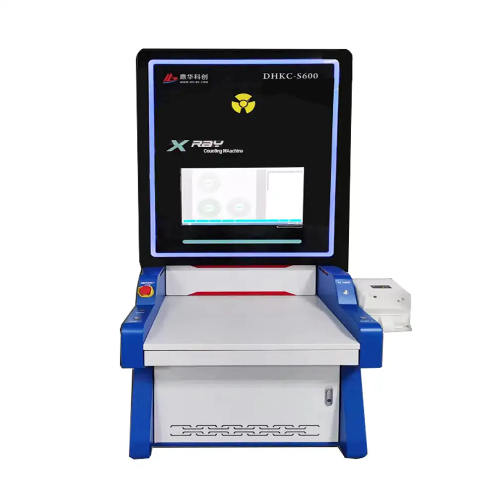
In high-mix, low-volume SMT manufacturing, manual component counting is a major bottleneck that drains labor hours and introduces costly inventory discrepancies. The Dinghua X-ray Counter Machine completely revolutionizes your warehouse management. By utilizing advanced industrial X-ray imaging combined with AI deep-learning algorithms, this system allows operators to calculate the exact component count of full SMD reels, tubes, or trays in seconds—without ever breaking the factory moisture-barrier seal.

Complete Guide to BGA Rework Station 2026: Tips for PCB Repair & Manufacturing
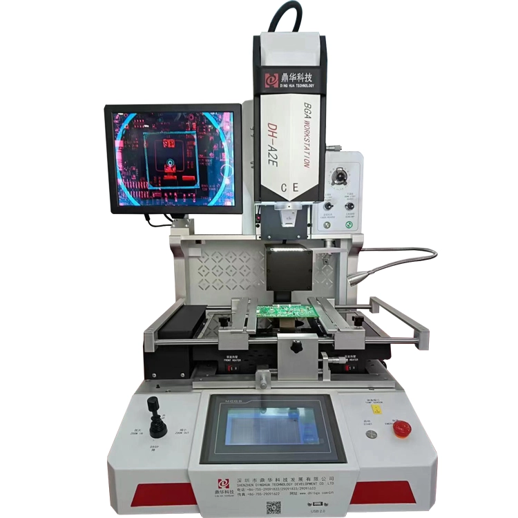
This 2026 guide covers everything you need to know about BGA rework stations, from core definitions to selection, operation, and maintenance. We draw on 15 years of hands-on experience manufacturing and testing BGA rework equipment, plus data from leading electronics industry associations to deliver unbiased, actionable advice. You’ll find step-by-step guides, comparison data, and answers to common questions to help you choose or use your BGA rework station correctly.

Complete Guide to Nondestructive Testing Equipment for Electronics Quality Control 2026
This comprehensive 2026 guide covers core knowledge of Nondestructive Testing Equipment, from basic definitions to practical selection and application tips, with a focus on the electronics manufacturing industry. We share hands-on testing insights, comparison data, and expert recommendations from our 15+ years of NDT manufacturing experience to help you find the right solution.
2026 Complete Guide to BGA Rework Station: Types, Uses & Buying Tips
This 2026 expert guide covers every critical aspect of BGA rework stations, from basic definitions and core components to step-by-step processes, model comparisons, and buying guidance. We draw on 12 years of hands-on testing and manufacturing experience from www.xraybgamachine.com, align with global IPC and RoHS standards, and answer common questions professionals have when purchasing a new station. This guide helps you make an informed buying decision for any facility size.


Contact Us
> Tel: +8615768114827 /+86-755-29091822
> Fax: +86-0755-29091622
> Email: John@dh-kc.com
> Address: 4th Floor, Building 6B, Shengzuozhi Technology Park, Xinqiao(518125),Bao'an,Shenzhen, Guangdong, China.

Copyright © 2024 Shenzhen Dinghua Innovation Technology Co., Ltd. All Rights Reserved.